
SEMICON West 2026Products & Services FLATSCAN thin film stress measuring system
FLATSCAN thin film stress measuring system
Exhibitor
OEG GmbH
FLATSCAN serves for the non-contact measurement of flatness, surface curvature, mean radius, and thin-film stress on all types of reflective surfaces—such as silicon wafers, mirrors, or even X-ray optics (Göbel mirrors). The measurement principle is based on measuring the reflection angle of a perpendicularly incident laser beam. The surface form can be precisely calculated from the change in the reflection angle between individual equidistant measurement points. For applications in semiconductor technology, thin-film stress (wafer stress) within coatings can be calculated based on the radii measured before and after the coating process.
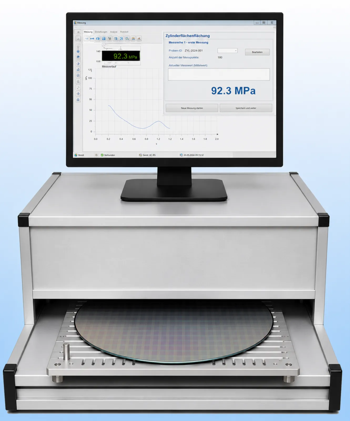
FLATSCAN 300