
OEG GmbH
Booth number: 1444-16
www.oeggmbh.com
About us
OEG GmbH is an internationally recognized provider of high-precision automatic optical measuring machines designed to capture optical, geometric, and physical parameters. Since 1991, the German-based engineering company has successfully covered the entire value chain in-house – including optical design, precision mechanical construction, electronics, and custom software development.
At SEMICON West, OEG highlights its cutting-edge metrology and quality control solutions for advanced semiconductor manufacturing:
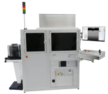
SURFTENS WH 300: The fully automatic flagship contact angle measuring instrument, equipped with an integrated wafer robot, load port, and SECS/GEM interface for seamless fab integration.
EBR Measurement: Add-on or standalone modules for precise evaluation of Edge Bead Removal efficiency.
Waferstress Systems: High-precision metrology for measuring mechanical thin-film stress on wafers.
MR200: A highly popular, industry-proven precision wafer scriber for 200mm wafers used worldwide.
With systems successfully installed across all continents, OEG is a trusted partner for global semiconductor manufacturers and advanced research institutes looking for uncompromising measurement accuracy and custom flexibility.
Product Categories: Metrology, Inspection & Test Equipment; Wafer Handling & Automation; Process Control Systems; Quality Assurance.
Address
Wildbahn 8i
15236 Frankfurt (Oder)
Germany
E-mail: info@oeggmbh.com
Phone: +49 335 5213894
Internet: www.oeggmbh.com
5302 Snapfinger Woods Drive
GA 30035 Decatur
United States
E-mail: jpress@classoneequipment.com
Phone: +1 612 227-5029
Internet: www.ClassOneEquipment.com
Contact person:
Dr.-Ing. Stephan Rothe
E-mail: s.rothe@oeggmbh.com
Phone: +49 335 5213894
Products & Services
OEG GmbH is an internationally recognized provider of high-precision automatic optical measuring machines designed to capture optical, geometric, and physical parameters. Since 1991, the German-based engineering company has successfully covered the entire value chain in-house – including optical design, precision mechanical construction, electronics, and custom software development.
At SEMICON West, OEG highlights its cutting-edge metrology and quality control solutions for advanced semiconductor manufacturing:
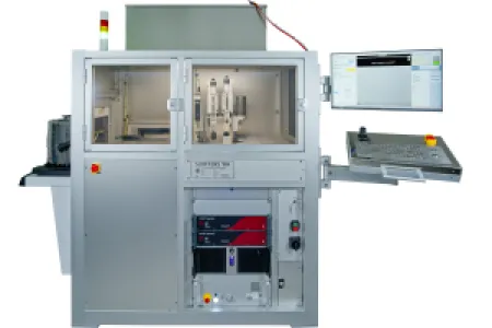
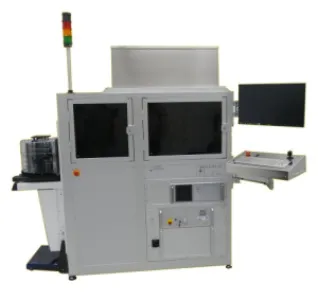
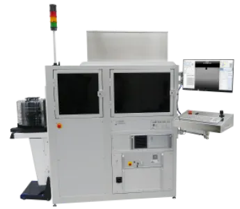
SURFTENS WH 300: The fully automatic flagship contact angle measuring instrument, equipped with an integrated wafer robot, load port, and SECS/GEM interface for seamless fab integration.
EBR Measurement: Add-on or standalone modules for precise evaluation of Edge Bead Removal efficiency.
Waferstress Systems: High-precision metrology for measuring mechanical thin-film stress on wafers.
MR200: A highly popular, industry-proven precision wafer scriber for 200mm wafers used worldwide.
With systems successfully installed across all continents, OEG is a trusted partner for global semiconductor manufacturers and advanced research institutes looking for uncompromising measurement accuracy and custom flexibility.
Product Categories: Metrology, Inspection & Test Equipment; Wafer Handling & Automation; Process Control Systems; Quality Assurance.
SURFTENS WH 300 fully automatic contact angle goniometer
Surface tension of photolithographic materials like resist and developer has a great potential for the photolithographic process itself. For instance, homogeneity of spin coatings, planarization, and adhesion depend directly on surface tension of the materials involved. The SURFTENS WH 300 contact angle meter serves for the measurement of contact angle and surface free energy (SFE) in semiconductor technology and provides the complete functionality, which is required in 300mm wafer fab´s. This makes the device unique worldwide
Main features of SURFTENS WH 300
-3 axis wafer handling robot
-load port for 12”-Wafer FOUP
-SECS / GEM interface
-optional bridge tool for 200mm FOUP
-video system for automatic drop shape analysis
-wafer scanner
-centring & notching before measurement
-automatic, software-controlled dosing system
-tank for main dosing system (DI water)
-automatic, software-controlled refill of main dosing system
-optional second dosing system for other test liquids
-filter fan unit
-optional hotplate for evaporating of water drops
-optional additional optical sensor for resist edge analysis
- single cable connection to the main power distribution unit of the instrument
- EMO is integrated
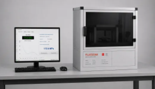
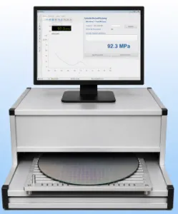
FLATSCAN thin film stress measuring system
FLATSCAN serves for the non-contact measurement of flatness, surface curvature, mean radius, and thin-film stress on all types of reflective surfaces—such as silicon wafers, mirrors, or even X-ray optics (Göbel mirrors). The measurement principle is based on measuring the reflection angle of a perpendicularly incident laser beam. The surface form can be precisely calculated from the change in the reflection angle between individual equidistant measurement points. For applications in semiconductor technology, thin-film stress (wafer stress) within coatings can be calculated based on the radii measured before and after the coating process.
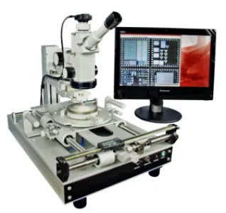
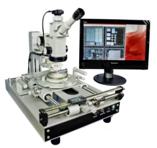
Precision wafer scriber MR 200
The setup and the equipment of MR 200 enable high precision scribing for defined cutting of structured silicon wafers. The MR 200 is an indispensable tool, in particular for REM preparations in semiconductor technology. The MR 200 is also suited for singling of chips in low numbers, for example in laboratory use.
EBR Measuring System
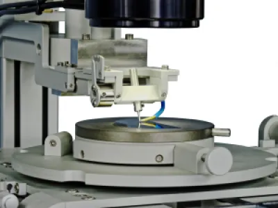
Applying photoresist, anti-reflective or polyimide coating to microelectronic substrates by spin coating often leads to the formation of so-called edge beading. This is the unwanted accumulation of the coated material on the outer edges of the substrate in the form of a bump. These accumulations can also wrap around the edge of the substrate and thereby also contaminate the edges of the back side of the substrate. If the edges of the wafers are not cleaned, the dried particles or photoresist residues can flake off, causing particle contamination and other problems in subsequent manufacturing and process steps. Therefore, the unwanted residues on the outer areas of the substrate should be removed. Special devices exist for this purpose.
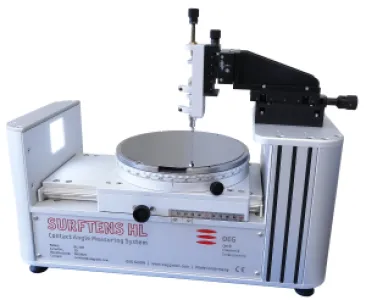
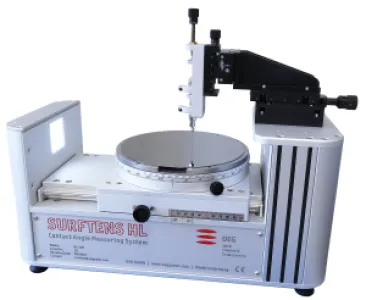
SURFTENS HL 200 - manual contact angle goniometer
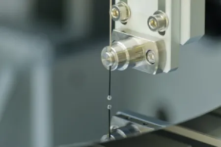
Surface tension of photolithographic materials like resist and developer has a great potential for the photolithographic process itself. For instance, homogeneity of spin coatings, planarization, and adhesion depend directly on surface tension of the materials involved. The same applies to the surface free energy (SFE) of coatings.
Surface free energy (SFE) of substrates and layers, used in semiconductor technology can be investigated by contact angle measurement. Measuring the contact angle allows you to quickly optimize new process steps as well as to better standardize known processes. Small changes in the surface property of wafers are seen as large, easily detected changes in the contact angle. A small investment of time to measure the contact angle, can give a large return by avoiding later production problems. To reduce defect density and feature sizes of resist structures (<1μm), a good adhesion of the resist is necessary. By the help of contact angle measurement, you can control the adhesion very easily.
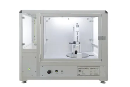
SURFTENS HL 200 is characterized by the following features
-compact space-saving, closed mechanical basic setup
-high quality measuring objective, fixed focus
-USB camera
-all components are integrated in a closed housing and protected against misalignment
-homogeneous, bright LED lighting, adjustable
-wafer table, 200mm diameter, Teflon-coated
-manual positioning of wafer table in x- and phi-direction
-wafer can be placed by vacuum tweezers
-stroke of wafer table: 100mm
-rotation of wafer table: 360°
This construction allows any point on the wafer surface to be measured.
The manual x and phi axes of the wafer-table are equipped with a scale so that defined positions can be approached.
Adjustments for dosing system(s):
--manual z-axis for adjustment of needle position (height)
--manual y-axis for adjustment of needle position (centring)
--manual x-axis for adjustment of needle position (focus)
Possible configuration of dosing system(s):
-one manual direct dosing system
-two manual direct dosing systems
-one automatic, software-controlled direct dosing system
-two automatic, software-controlled direct dosing systems
-combination of one manual and one automatic, software-controlled direct dosing systems