
3D-Micromac AG
Booth number: 1245-08
3d-micromac.com
About us
3D-Micromac AG is a leading provider of laser micromachining systems for high-precision applications in semiconductor manufacturing and advanced electronics. The company offers innovative laser solutions for key processes, including
Laser dicing,
Ohmic Contact Formation (OCF) on SiC power devices,
Selective reference layer pinning in TMR and GMR sensors,
Adjustment and calibration of integrated circuits (laser link trimming
Laser drilling for TSV and TGV applications,
Laser-based sample failure analysis (FA) and quality assurance (QA).
Its system platforms—such as the microPRO™ XS OCF for laser annealing of SiC wafers for power devices, the microVEGA® platform for selective laser annealing and laser link trimming processes, and the microPREP® systems for precise and efficient sample preparation in failure analysis, quality assurance and materials research—are engineered to deliver process reliability, flexibility, and optimal results at the micro- and nanoscale.
Headquartered in Chemnitz, Germany, 3D-Micromac combines cutting-edge laser technology with deep process expertise and strong global customer support to address the evolving needs of the semiconductor and electronics industries.
Address
Technologie-Campus 8
09126 Chemnitz
Germany
E-mail: info@3d-micromac.com
Phone: +49 371 400430
Internet: 3d-micromac.com
780 Montague Expy #306
CA 95131 San Jose
United States
E-mail: stearns@3d-micromac.com
Phone: +1 603 305-4263
Contact person:
Joshua Stearns
GM Sales & Business Development US East
E-mail: stearns@3d-micromac.com
Phone: +1 603 305 4263
Christian Wolf
Director, Business Development and Operations | General Manager
E-mail: c.wolf@3d-micromac.com
Phone: +1 408 858 0107
Daniel Weber
Area Sales Manager
E-mail: weber@3d-micromac.com
Phone: +49 371 40043 995
Products & Services
3D-Micromac offers innovative laser solutions for key processes, including lase dicing, Ohmic Contact Formation (OCF) for SiC power devices, selective reference pinning in TMR and GMR sensor, ultra-high precision laser processing, and laser-based sample preparation for failure analysis and quality assurance.
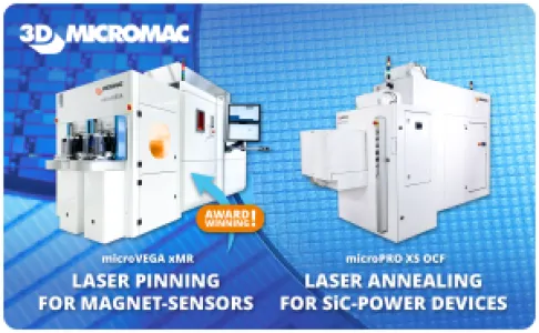
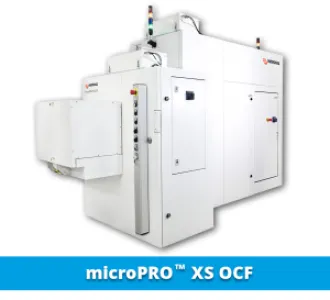
Laser Annealing for SiC Power Devices: microPRO XS OCF
Selective laser annealing enables targeted activation of functional layers with minimal thermal impact on surrounding structures – a key technology in advanced semiconductor production. Our systems offer outstanding process uniformity, repeatability, and efficiency at an industrial scale.
The microPRO XS OCF enables accurate activation of ohmic contacts on SiC wafers for power device applications. It delivers application-optimized annealing at the highest technological level while keeping CoO low.
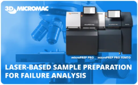
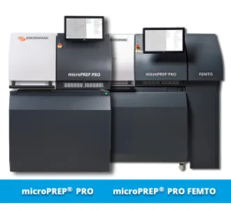
Laser-based Sample Preparation for FA: microPREP® PRO and microPREP® PRO FEMTO
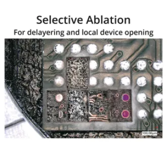
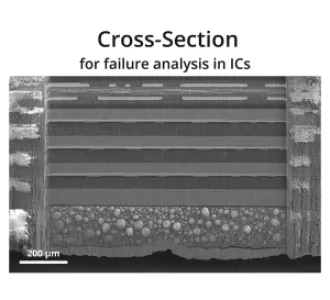
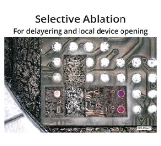
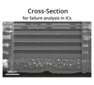
microPREP® PRO FEMTO is 3D-Micromac’s high-precision laser ablation system specifically engineered for advanced sample preparation tasks in semiconductor failure analysis and device characterization. Equipped with a femtosecond laser, it enables high-resolution cross-sectioning and delayering with minimal thermal or mechanical impact—ideal for the preparation of complex, multilayer semiconductor structures.
Unlike conventional methods such as mechanical polishing or ion beam milling, microPREP® PRO FEMTO uses ultrashort laser pulses to selectively remove material while preserving structural integrity and analytical fidelity. Compared to FIB systems, the laser-based process is significantly faster, especially when preparing larger areas or coarse material removal is required. This makes it a powerful, non-destructive and time-saving alternative—or complementary front-end tool—to traditional FIB and other established preparation techniques.
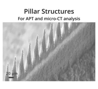
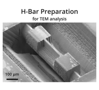
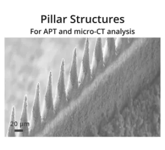
The system is also capable of processing larger samples and packages, supporting a broad range of specimen geometries and materials—including metals, semiconductors, ceramics, polymers, and advanced composites. A user-friendly software environment with predefined workflows ensures reproducibility and integration into existing analysis workflows such as SEM, TEM, APT, X-ray tomography, and micromechanical testing.
By reducing time-to-sample and minimizing tool bottlenecks, microPREP® PRO FEMTO increases throughput, lowers cost of ownership, and enhances lab efficiency—especially in semiconductor labs dealing with growing sample volumes and complexity.
Laser Annealing: Selective reference-layer pinning for advanced monolithically integrated sensor TMR / GMR sensor concepts
Magnetic sensors are a key enabling technology for automotive, industrial, consumer and emerging medical/HMI applications. Driven by demand for higher sensitivity, lower power consumption, smaller footprints and greater integration, TMR sensors are gaining relevance.
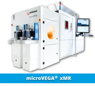
Translating this potential into monolithically integrated sensor layouts – from Wheatstone bridges to angle and multi-axis concepts – requires local definition of sensor sensitivity axes at wafer level. Selective laser-based reference-layer pinning provides this capability by combining a selective laser spot with a local magnetic field, allowing defined sensor areas to be pinned in the desired direction – with additional relevance for GMR sensors.
microVEGA™ xMR is a production-proven platform used in 24/7 high-volume fabs worldwide. It combines localized thermal impact, recipe-based flexibility and on-the-fly processing for cost-efficient production of next-generation TMR/GMR sensor architectures.
Laser Link Trimming: Ensuring fail-safe integrity and long-term robustness of analog, power-management & mixed signal ICs through permanent hardware configuration
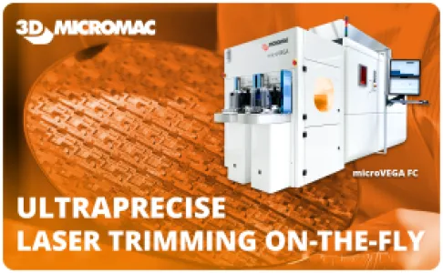
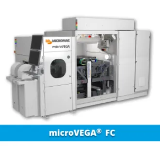
Laser Link Trimming (LLT) enables permanent hardware configuration for analog, power-management and mixed-signal ICs in automotive, industrial, aerospace and other high-reliability applications. Typical devices include gate drivers, BMS ICs and high-side switches, where LLT supports variant configuration and permanent hardware limits for safety-critical and fail-safe functions.
Complementing rewritable NVM, Trim-DACs and electrically programmed OTP solutions, LLT creates irreversible, tamper-resistant configurations by modifying predefined metal links – without electrical programming stress or the need for dedicated memory structures.
microVEGA™ FC enables high-throughput wafer-level LLT on a production-grade platform for semiconductor manufacturing, combining ±200 nm positioning accuracy (3σ), closed-loop process control and on-the-fly processing at up to 400 mm/s for an exceptional balance of speed, precision and process stability.
Laser-Based Sample Preparation on Full-Wafer- and Board-Level
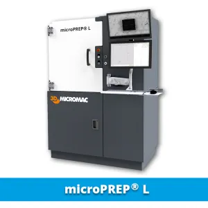
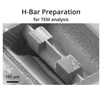
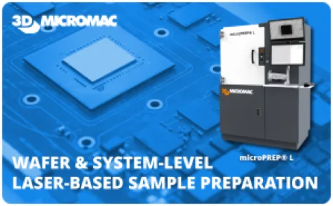
Our field-proven microPREP® systems accelerate sample preparation for a wide range of failure analysis methods, including TEM, SEM, APT, XRM, and micromechanical testing. The latest development, the microPREP® L, can prepare specimens on bigger samples like 12” wafers or system-level boards. These can even be prepared across multiple areas of the same sample in a single run, without process restarts.
Free your FIB/SEM for what it does best – speed up your time-to-sample with laser-based sample preparation with microPREP® systems.