3D-Micromac AG
Booth number: 1261-5
3d-micromac.com
About us
3D-Micromac AG is a leading provider of laser micromachining systems for high-precision applications in semiconductor manufacturing and advanced electronics. The company offers innovative laser solutions for key processes, including Ohmic Contact Formation (OCF), magnet sensor pinning, laser link trimming, and sample preparation for failure analysis. 3D-Micromac also holds extensive expertise in the processing (cutting, drilling, ablating) of various materials (Si, SiC, glass, stacks) used in the semiconductor industry.
Its system platforms—such as the microPRO™ XS OCF for laser annealing of SiC wafers for power devices, the microVEGA® platform for selective laser annealing and laser link trimming processes, and the microPREP® PRO for precise and efficient sample preparation in failure analysis and materials research—are engineered to deliver process reliability, flexibility, and optimal results at the micro- and nanoscale.
Headquartered in Chemnitz, Germany, 3D-Micromac combines cutting-edge laser technology with deep process expertise and strong global customer support to address the evolving needs of the semiconductor and electronics industries.
Address
Technologie-Campus 8
09126 Chemnitz
Germany
E-mail: info@3d-micromac.com
Phone: +49 371 400430
Internet: 3d-micromac.com
780 Montague Expy #306
CA 95131 San Jose
United States
E-mail: stearns@3d-micromac.com
Phone: +1 603-305-4263
Contact person:
Joshua Stearns
GM Sales & Business Development US East
E-mail: stearns@3d-micromac.com
Phone: +1 603 305 4263
Products & Services
3D-Micromac offers innovative laser solutions for key processes, including Ohmic Contact Formation (OCF), magnet sensor pinning, laser link trimming, and sample preparation for failure analysis.
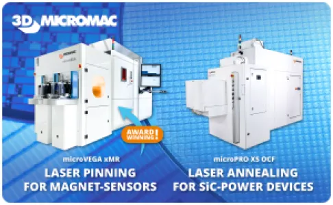
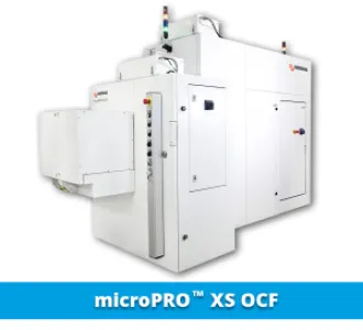
Laser Annealing for SiC Power Devices: microPRO XS OCF
Selective laser annealing enables targeted activation of functional layers with minimal thermal impact on surrounding structures – a key technology in advanced semiconductor production. Our systems offer outstanding process uniformity, repeatability, and efficiency at an industrial scale.
The microPRO XS OCF enables accurate activation of ohmic contacts on SiC wafers for power device applications. It delivers application-optimized annealing at the highest technological level while maintaining a low CoO.
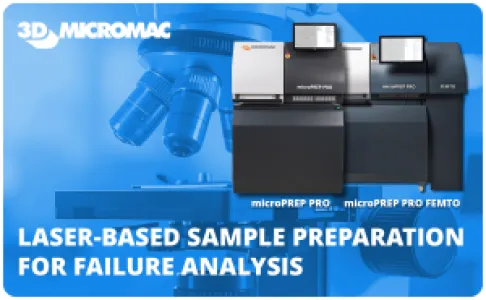
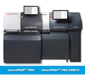
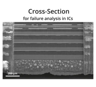
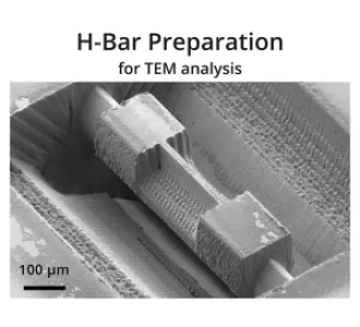
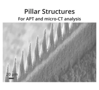
Laser-based Sample Preparation for FA: microPREP® PRO and microPREP® PRO FEMTO
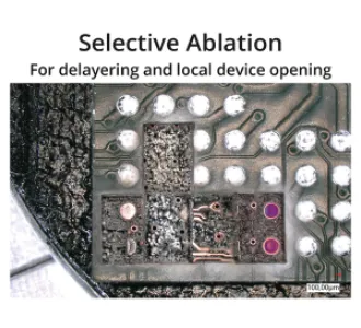
microPREP® PRO FEMTO is 3D-Micromac’s high-precision laser ablation system engineered explicitly for advanced sample preparation tasks in semiconductor failure analysis and device characterization. Equipped with a femtosecond laser, it enables high-resolution cross-sectioning and delayering with minimal thermal and mechanical impact, making it ideal for preparing complex, multilayer semiconductor structures.
Unlike conventional methods such as mechanical polishing or ion beam milling, microPREP PRO FEMTO uses ultrashort laser pulses to selectively remove material while preserving structural integrity and analytical fidelity. Compared to FIB systems, the laser-based process is significantly faster, especially when preparing larger areas or coarse material removal is required. That makes it a powerful, non-destructive, and time-saving alternative—or complementary front-end tool—to traditional FIB and other established preparation techniques.
The system is also capable of processing larger samples and packages automatically, supporting a broad range of specimen geometries and materials, including metals, semiconductors, ceramics, polymers, and advanced composites. A user-friendly software environment with predefined workflows ensures reproducibility and seamless integration into existing analysis workflows, including SEM, TEM, APT, X-ray tomography, and micromechanical testing.
By reducing time-to-sample and minimizing tool bottlenecks, microPREP PRO FEMTO increases throughput, lowers the cost of ownership, and enhances lab efficiency, particularly in semiconductor labs that deal with growing sample volumes and increasing complexity.
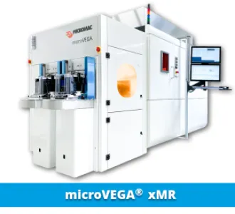
Magnet Sensor Pinning: microVEGA® XMR
Selective laser annealing enables targeted activation of functional layers with minimal thermal impact on surrounding structures – a key technology in advanced semiconductor production. Our systems offer outstanding process uniformity, repeatability, and efficiency at an industrial scale.
Our award-winning microVEGA xMR precisely aligns magnetic layers for GMR and TMR sensors and is used worldwide in the high-volume production of monolithically integrated sensor chips.
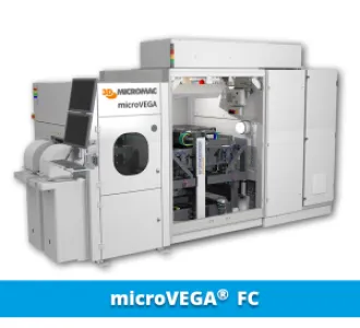
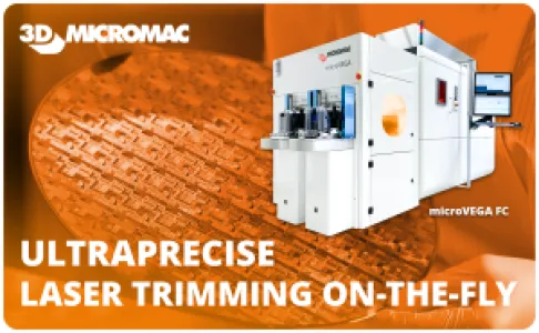
Ultra-precise On-The-Fly Laser Processing: microVEGA® FC
3D-Micromac designed the microVEGA FC system for high-precision laser processing of semiconductor wafers during continuous motion. With 3D calibration, dynamic focus correction, and a positioning accuracy of 150 nm at 400 mm/s, the system delivers top-level precision at the highest throughput.
It combines speed, accuracy, and stability for the most demanding laser processing tasks. Its user-friendly control and seamless integration into existing production lines ensure maximum availability and support long-term process efficiency while keeping unit costs low.
Typical applications include trimming digital potentiometers, programming logic structures, or repairing embedded memory cells—but a lot more is imaginable. Let's get in contact to discuss your application that needs ultra-precise laser processing.