Precitec 3D Metrology
Booth number: 1261-18 + 1261-19
www.precitec.com
About us
PRECISION MEASUREMENT IN SEMICON APPLICATIONS
Precitec 3D Metrology – enabling precision from wafer to package
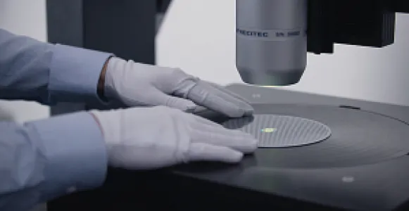
In everything from wafer production to device packaging, Precitec harnesses the power of light to offer state-of-the-art real-time measurement solutions in the sub-micro range based on chromatic confocal technology, interferometric technology and laser photothermal technology. Our non-destructive, non-contact metrology solutions cover critical parts of the semiconductor production process and relevant materials such as silicon, gallium arsenide, indium phosphide and silicon carbide.
Precitec offers high-precision measurement solutions for the following applications:
· High-speed wafer inspection: Fast wafer sorting by TTV, bow and warp, even of challenging geometries
· Wafer cleaning: Monitoring multiple wafer cleaning processes
· Back end: Measuring adhesive thickness and micro-bumps and detecting voids in bonding
· High-precision levelling and wafer & photomask alignment
· Ceramic carbide coatings: Extending maintenance levels for a faster ROI
-thumb.webp)
Address
Schleussnerstrasse 54
63263 Neu-Isenburg
Germany
E-mail: c.meerman@precitec-optronik.de
Phone: +49 61023676125
Internet: www.precitec.com
4000 Burton Dr.
CA 95954 Santa Clara
United States
E-mail: v.tran@precitec.com
Phone: +1 (248) 305 1667
Internet: precitec.com
28043 Center Oaks Ct.
MI 48393 Wixom
United States
E-mail: precitec@precitec.com
Phone: +1 (248) 446 8100
Internet: precitec.com
Contact person:
Dr. Oliver Schulz
Director of Business Development Semiconductor
E-mail: O.Schulz@precitec-optronik.de
Phone: +49 6102 3676 182
Vinh Tran
Sales & Applications Manager West Coast
E-mail: V.Tran@precitec.com
Phone: +1 (408) 207 5011
Salvatore Marinello
Eastern Regional Sales Manager
E-mail: S.Marinello@precitec.com
Phone: +1 248 978 6632
Georg Tank
Business Development Manager Metrology
E-mail: G.Tank@precitec.com
Phone: +1 630 441 7229
Products & Services
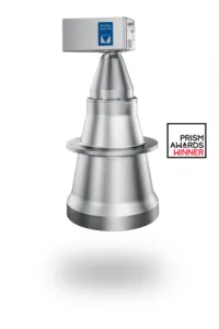
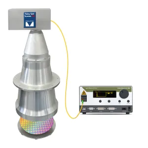
High-Speed OCT Metrology for Semiconductor Quality Control – Precitec Flying Spot Scanner 310
Flying Spot Scanner 310 + CHRocodile 2 IT
Winner of the SPIE Prism Award 2023
High-speed OCT system for precise measurement of distance, thickness, and topography.
Rotary scanning replaces linear motion for unmatched speed and accuracy.
Key Features:
• Simultaneous TTV, bow, and warp data in one scan
• No moving axes – robust, fast, and precise
• Ideal for in-line semiconductor quality control
Engineered for demanding metrology tasks where precision is critical.
Experience award-winning performance – Flying Spot Scanner 310.
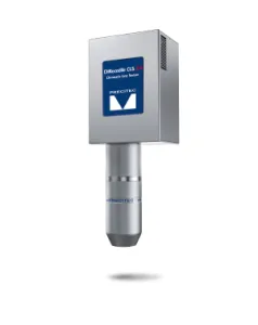
CHRocodile CLS 2 – High-Speed Confocal Line Sensor for 3D Surface Metrology
Precitec’s CHRocodile CLS 2 is a powerful confocal line sensor delivering fast, non-contact 3D measurements with submicron precision. Ideal for in-line inspection in semiconductor and electronics manufacturing, it captures full profiles at up to 384,000 3D points per second.
Key Benefits:
• High-speed acquisition for real-time process control
• Precise 3D data on surface, thickness, and step heights
• Robust, compact design for industrial integration
Optimize quality control with reliable, high-throughput metrology.
CHRocodile CLS 2Pro – High-Speed Confocal Line Sensor with Unmatched NA and Line Length
The Line Sensor CLS 2Pro sets a new benchmark in high-speed 3D inspection. With a unique 8 mm line length and 38° acceptance angle, it combines wide coverage with exceptional lateral resolution.
Key Specs:
• 36,000 lines/sec scan speed
• 21 million points/sec
• No shadowing – ideal for complex geometries
Designed for precision, speed, and reliability in semiconductor and electronics metrology.
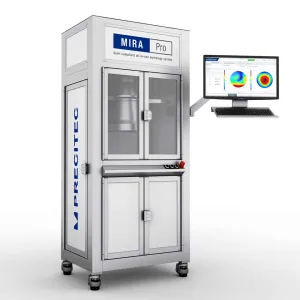
MIRA Pro - semi-compliant, all-in-one metrology system
MIRA Pro combines Precitec’s award-winning Flying Spot Scanner 310 with an all-in-one platform for precise measurement of TTV, bow, and warp.
Ideal for:
• Semiconductor labs, R&D, and universities
• Off-line inspection and quality control
• Versatile use across wafer types and materials
Fully equipped with hardware and software – ready for immediate deployment in advanced metrology tasks.
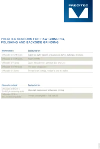
In-Process Wafer Thickness Monitoring for Grinding Applications
Precitec’s 3D metrology solutions enable precise, non-contact thickness control during wafer thinning and structuring – even in harsh environments with grinding slurry.
Key Advantages:
• Accurate TTV measurement across wide thickness/material ranges
• Suitable for Si, SiC, GaN, InP, sapphire, LiTaO, and more
• Water-/acid-resistant probes and water jet sensors for low maintenance
• Designed for seamless OEM integration into process tools
Ensure consistent quality and reduce costs with robust in-line metrology.