Fabmatics GmbH
Booth number: 1261-11
www.fabmatics.com
About us
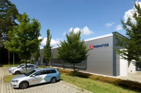
Fabmatics, headquartered in Dresden, Germany, is an experienced specialist for the automation of material flows and handling processes in semiconductor factories, semiconductor process plants and other high-tech production environments.
Founded in 1991, the company has been successfully implementing customer-specific automation projects in the semiconductor industry for almost 35 years. This results in a strong market position, especially in the modernization of legacy semiconductor factories worldwide.
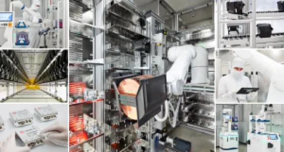
Fabmatics has the unique competence to offer comprehensive automation, robotics and handling systems for use under cleanroom conditions, including both hardware and software, from consulting, simulation and development to production, installation and after-sales service from a single source. Our product portfolio includes mobile robots, robot cells, automated transport and storage systems, purge solutions, product identification systems and more.
Fabmatics, including its subsidiary Fabmatics USA Inc. in Utica (New York), is world-wide active and employs at present approximately 320 employees. Fabmatics is a proud member of the SCIO Automation Group, which employs 1,800 people across eight countries. Together, we deliver smart factory automation solutions to global leaders and hidden champions in a wide range of industries.
Fabmatics is member in the world-wide industry association SEMI, in the high-tech network Silicon Saxony and in the Automation Network Dresden (AND).

Address
Zur Steinhöhe 1
01109 Dresden
Germany
E-mail: info@fabmatics.com
Phone: +49 351 652370
Internet: www.fabmatics.com
326 Broad St., Suite 1
NY 13501 Utica
United States
E-mail: info.usa@fabmatics.com
Phone: +1 315 316 1480
Internet: www.fabmatics.com
Contact person:
Products & Services
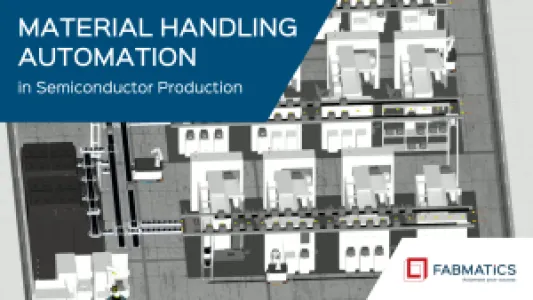
Innovative Ideas for Material Handling Automation
Our engineers are constantly researching potential improvement in the area of factory automation and developments for innovative and competitive products, which keep your material flow moving optimally. We support you in the following areas:
Identification:
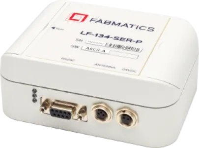
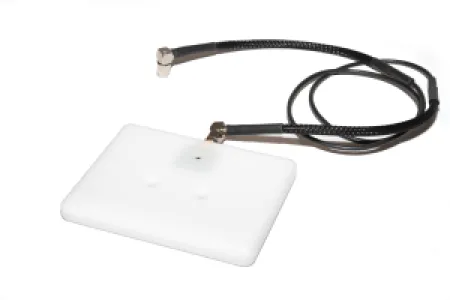
RFID Retrofit (Tag Welding on Cassette, Tool Integration, RFID Retrofit for Stockers, Racks, Transport Systems)
RFID Components (LF-, HF Readers, Antennas, Accessories)
RFID Logistic Systems (Racks, Carts, Reading Stations)
Indoor GPS (Localization)
Transport:
Conveyor Systems
Overhead Hoist Transfer
OHT Interfaces
Lifts
PGVs, AGVs
Handling:
Mobile Robots
Robot Cells
EFEMs
Storage:
Floor Stockers
Zero Footprint Stockers
Test Wafer Center
Protection:
Wafer Pod Purge Systems
Consulting:
Fab Assessment & Feasibility Studies
Fab Simulation
Material Flow Optimization
Software:
System integration
Fleet Management
GUI Development
Service:
24/7 System Support, Preventive Maintenance, Spare Parts Management, Upgrade Services
Third Party Support
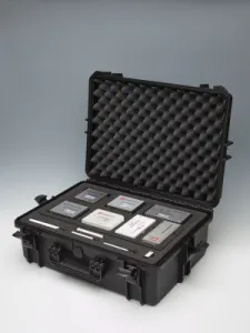
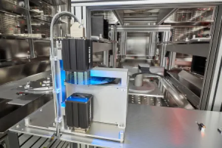
Fit for Automation - RFID Solutions as Key Enabler for Automated Semiconductor Manufacturing
In semiconductor manufacturing, automation begins with reliable digital identification. Even small steps - like tagging carriers or enabling tools to communicate - can significantly increase transparency, reduce errors, and lay the foundation for smarter logistics and scalable process automation. Many fabs still rely on manual or paper-based tracking, making it harder to evolve.
That’s where Fabmatics comes in: With over 20 years of industry experience, we help you take the first step—fitting RFID solutions to your fab’s infrastructure, goals, and pace.
Whether you're retrofitting an existing fab or building new – our RFID systems are scalable, SEMI-compliant, and made to integrate.
Retrofit-ready
LF & HF RFID hardware for cleanrooms
Tailored for FOUPs, SMIF pods, HA200 boxes, Open Cassettes, Reticle Carriers
Full integration into MES and fab infrastructure
-thumb.webp)
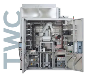
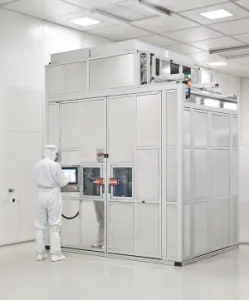
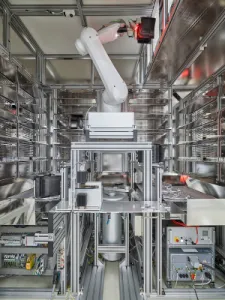
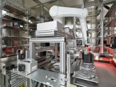
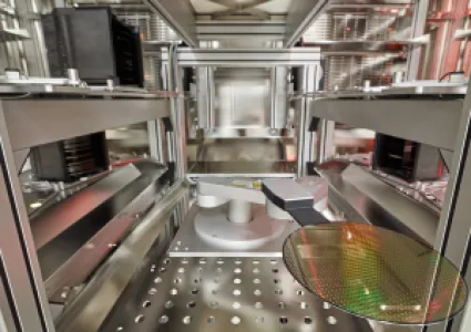
Test Wafer Center - The all-in-one Test Wafer Managment Solution
Test wafers are indispensable for semiconductor manufacturing, crucial for equipment qualification and process monitoring. They constitute up to 50% of a fab’s wafer inventory. Managing test wafer lots manually is time-consuming and prone to errors.
The Test Wafer Center (TWC) fully automates kitting and de-kitting of test wafer lots as well as their storage. Its compact and highly flexible layout allows up to 93 storage bins and up to 14 material handling locations making it the perfect solution for complex equipment qualifications scenarios. It gives you complete (remote) control for determining timing and content of each test wafer lot & enables just-in-time delivery to your process equipment.
Featuring SECS host communication, camera-based robot routing, optional wafer alignment & identification, and various carrier identification options, the TWC ensures safe, accurate, & fully traceable material control.
Connecting to any Automated Material Handling System (conveyor or vehicle based) as well as allowing manual carrier input or output, the integration with your fab is seamless & quick.
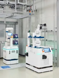
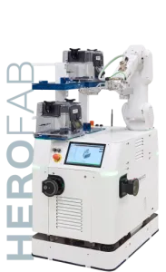
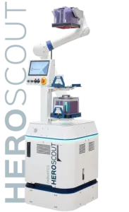
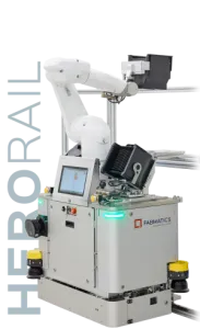
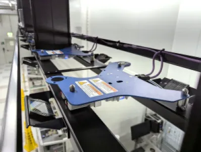
Mobile Robots - Meet the Fabmatics HERO family!
Our field-proven fleet of mobile robots - our HERO's - are your perfect match for the handling and transport of wafers, reticles and carriers in the semiconductor industry, as well as for similar substrates in micro and nanoelectronics. They make manual intervention superfluous, helping you to optimize the material flow in your fab.
Navigating their way either autonomously, track- or rail-bound through semiconductor fab's wordwide, they truly are heroes in the cleanroom and make sure that the right material arrives at the right time.
Explore how our automation solutions fit into your manufacturing environment and elevate your fab’s performance, setting new standards for productivity and competitiveness.
HERO Family:
HERO Fab: Automated guided vehicle (AGV) for quick transport and automatic handling of 200mm wafer cassettes or 300mm FOUPs
HERO Scout: Autonomous mobile robot (AMR) for the automated handling and transportation of reticle pods
HERO Rail: Rail-guided vehicle (RGV) for the transport and automated handling of wafer cassettes
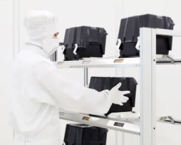
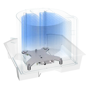
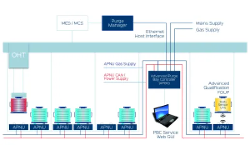
Wafer Pod Purge System - Reliable Wafer Protection During Interim Storage
Fabmatics’ retrofittable Purge System for FOUP and SMIF pods continuously purges wafer carriers with inert gas during interim storage – reliably protecting wafers between process steps from contamination, oxidation, and humidity-induced chemical reactions.
More than 18,000 Fabmatics purge units are already in operation worldwide.
Key Benefits
Reduces wafer defects and yield loss
by preventing airborne molecular contamination (AMC) and oxidation during storageExtends production flexibility
by allowing longer queue times between process steps without contamination riskImproves overall yield
through continuous wafer protection in non-active storage locationsLowers operational costs
with durable, low-maintenance components designed for long-term useProtects your existing infrastructure investment
by retrofitting seamlessly into current FOUP/SMIF pod storage systems like Zero Footprint StorageMaximizes cleanroom efficiency
with a compact design that requires no additional floor spaceEnsures full process visibility and control
via intelligent web-based monitoring and optional HSMS integration
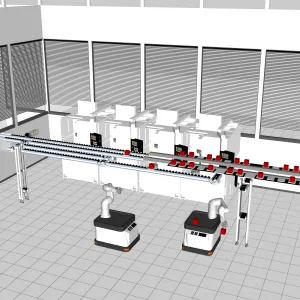
Material Flow Simulation - We make your System's Potential visible before it's built!
Material flow simulation is a powerful tool for analyzing and assessing existing system conditions or for enabling well-founded decisions in automation projects. Using material flow simulation, all relevant logistical processes of a semiconductor fab can be integrated into a single comprehensive and dynamic digital model.
The in-depth experimental analysis of this model allows for detailed insights and holistic conclusions about the existing underlying real-world system or can even be used for envisioning the potential dynamics of a non-existing system. This enables our developers and engineers to work with you to minimize risks in the project, create a better understanding of the system and support you effectively in the decision-making process.