
Vistec Electron Beam GmbH
Booth number: 1245-04
www.vistec-semi.com
About us
As a long-standing equipment supplier, Vistec Electron Beam GmbH is providing leading technology solutions for advanced electron-beam lithography. Based on the Variable Shaped Beam (VSB) principle, the electron-beam lithography systems are mainly utilized for semiconductor applications and advanced research as electron-beam direct write in semiconductor manufacturing, mask making as well as integrated optics and several new emerging markets.
For some time now Vistec’s Variable Shaped Beam systems are increasingly used as a direct write technology for Silicon as well as Compound Semiconductor based IC manufacturing. Using an advanced electron-beam writer in mix-and-match mode with an optical lithography system has proven itself as a practical and cost-effective solution for these applications. Especially in the Compound Semiconductor manufacturing market Vistec Electron Beam‘s systems have demonstrated their production capability & high system reliability also in 24 / 7 operation by double digit fab installations world wide.
Vistec Electron Beam´s roots go back to the 1950´s when the company was part of Carl Zeiss Jena where the first electron microscope was developed. In 1974, the first commercial Variable Shaped Beam system was launched. Vistec Electron Beam GmbH has been active on the market in its current structure since 1996. The company joined the HEIDENHAIN Corporate Group in 2012. Currently the company employs more than 100 people worldwide. 80% of its employees hold a degree in Physics or Technical Sciences and Engineering.
Located in Jena (Federal State Thuringia, Germany) the company benefits from the synergies between the university, leading edge research institutes, small and mid-size equipment and supplier companies as well as key semiconductor manufactures in the neighboring area. This provides excellent preconditions for a successful product development today and in the future.
In addition to its production facility in Germany, Vistec Electron Beam maintains service and support centers in Europe, Taiwan and in the US.
Address
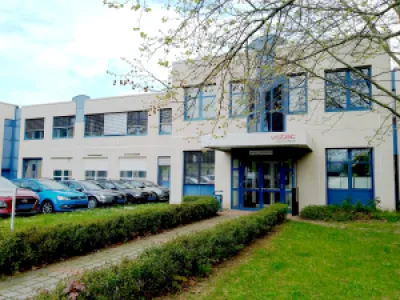
Ilmstr. 4
07743 Jena
Germany
E-mail: ines.stolberg@vistec-semi.com
Phone: +49 3641 77980
Internet: www.vistec-semi.com
Contact person:
Ines Stolberg
Manager Marketing & Sales
E-mail: ines.stolberg@vistec-semi.com
Products & Services
Vistec SB254
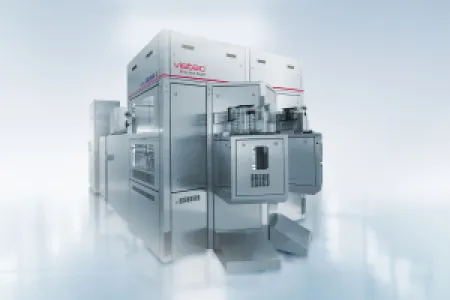
Vistec Electron Beam develops, manufactures, sells and services electron-beam lithography systems which are based on the Variable Shaped Beam (VSB) technology. The dedicated and tailored data preparation solution ePLACE (licenced by Vistec Electron Beam) ensures a perfect link between design and lithography performance. The portfolio covers electron-beam lithography systems with 200 mm and 300 mm platforms. This high flexibility gives access to a wide range of applications in R&D, prototyping, and small volume production.
The Vistec VSB systems combine state of the art fully automated substrate handling, adjustment and alignment with a high-precision stage system and a sophisticated electron-optical 50 keV column specifically developed to ensure excellent lithography performance. All Vistec systems featuring exposure strategies as “write-on-the-fly”, vector scan and multi-pass exposure.
Vistec’s SB254 is a fully automated, high performance, cost-effective electron-beam lithography system designed for use in both industry and advanced research. Based on the Variable Shaped Beam (VSB) principle, these tools are utilized in a wide range of existing and emerging semiconductor and nanotechnology applications including silicon direct write, compound semiconductor, mask making, integrated optics, and silicon photonics.

Vistec SB3050-2
The Vistec SB3050-2 is today’s most advanced Electron Beam Lithography system with Variable Shaped Beam technology and full writing capability on mask or wafer substrates of up to 300 mm dimension.
Effective writing techniques and Variable Shaped Beam electron optics make the simultaneous use of fast exposure and high resolution possible. The Cell Projection function improves throughput and pattern fidelity of repetitive or curvilinear structures.
Thanks to the production-compatible Graphical User Interface (GUI), the Vistec SB3050-2 can be easily integrated into automated production environments (CIM). Capable of exposing both masks (including templates) and wafers, the SB3050-2 exposure tools are ideal for bridging the gap between next-generation technology nodes.