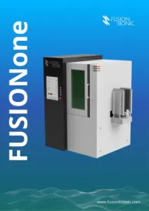

Fusion Bionic GmbH
Booth number: 1245-07
www.fusionbionic.com
About us
Fusion Bionic is revolutionizing laser structuring with DLIP technology for surfaces.
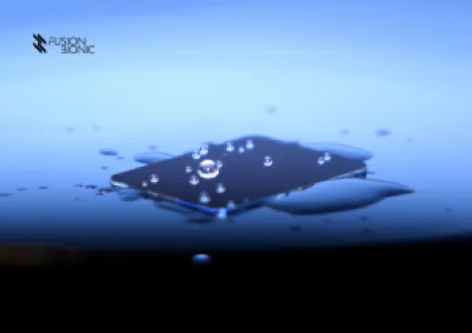
Our high-speed laser processes enable functions like thermal-management, underfilling, optimised bonding, tailored wettability, adhesion, anti-reflection and more.
Industries such as semiconductors, glass, consumer electronics and photovoltaics benefit from scalable, sustainable, and production-ready solutions.
From technology to production systems – we deliver customized turnkey solutions all from one source.
Whether integrated into existing lines or as stand-alone units: we bring function to material.
Address
Löbtauer Straße 69
01159 Dresden
Germany
E-mail: contact@fusionbionic.com
Phone: +49 351 16074068
Internet: www.fusionbionic.com
Contact person:
Dr. Tim Kunze
CEO
E-mail: contact@fusionbionic.com
Phone: +49 351 16074068
Products & Services
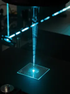
Fusion Bionic GmbH, located in Dresden, Germany, is a solution provider for laser-based surface functionalization. We develop laser solutions for large-area and high-speed surface processing using Direct Laser Interference Patterning (DLIP).
Our scalable platform technology creates defined micro- and nanostructures directly on silicon carbide, metals, polymers, ceramics, glass, and other technical materials in a fast, contactless, single-step process. Our expertise in material processing enables us to adapt surface properties precisely to the requirements of semiconductor and other high-tech applications.
Our turnkey and customized machine solutions combine coordinated laser and process technology with automation and integrated quality assurance. The systems can be adapted to customer-specific materials, component geometries, and production requirements.
Adjustable structure periods, ranging from the sub-micrometer scale to several tens of micrometers, combined with high processing speeds, allow both precision and industrial throughput to be matched to the application.
Applications include:
Thermal management
Increased effective contact area
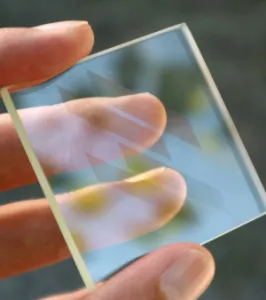
Engineered optical properties, including anti-reflection
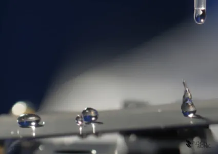
Controlled wettability
Bonding and debonding
Optimized adhesion
Improved underfilling
Visit Fusion Bionic at SEMICON West to discover how laser-engineered surfaces and scalable laser-processing solutions can improve the performance of next-generation semiconductor products.